
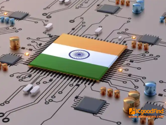
The Indian government has unveiled the implementation rules for Semicon 2.0 (India Semiconductor Mission 2.0), with a total subsidy pool of INR 1.275 trillion ($13.4B) . Unlike the 2021 program focused on fabs and packaging, the new policy extends support to chip design, semiconductor equipment, key materials, R&D, and talent development – aiming to build a full domestic semiconductor ecosystem.
Key policy shifts:
Chip design: Startups and SMEs in IC, SoC, and IP development can receive seed funding up to 50% of project cost (capped at INR 150M, ~$1.6M) under the DLI (Design Linked Incentive) program. Larger design houses with venture/private equity backing can opt for equity co‑investment or patent licensing financing for tape‑outs, commercialization, and IP operations.
Equipment and materials: First‑time subsidies for semiconductor manufacturing tools, refurbished equipment, subsystems, and core components – covering lithography, etching, vacuum systems, precision motion platforms, and RF components. Eligible players can receive up to 30% of qualifying capex , with additional PLI (Production Linked Incentive) benefits for some projects.
Talent: The government aims to train 100,000 semiconductor design engineers over the next five years, building on 85,000 already trained under Phase 1 – leveraging India's existing design‑engineer base (ARM, AMD, Intel, Qualcomm, MediaTek all have R&D centers in Bengaluru and Hyderabad).
Phase 1 legacy: The 2021 Semicon India program ($10B) attracted Micron (ATMP plant in Gujarat), Tata Group (wafer fab, OSAT, EMS projects), and established Gujarat as a semiconductor hub.
Semicon 2.0 expands the scope to six pillars: chip design, equipment & materials, wafer fabrication, advanced/legacy packaging, R&D, and talent development. The application window is open for three years, project execution up to six years, under the oversight of the India Semiconductor Mission (ISM).
Long‑term ambition: India targets a $110‑120B domestic semiconductor market by 2030 , attracting ~INR 4 trillion in private capital, and aims to build a self‑reliant design‑manufacturing‑packaging supply chain over the next six years.
ICgoodFind Takeaway:
India is moving beyond fab‑only incentives to design‑equipment‑talent full‑stack support. For a country with strong chip design talent but weak manufacturing, Semicon 2.0 is a bet on turning that talent into a self‑sustaining industrial base – a strategy that will take years to mature, but could reshape global supply chains.
